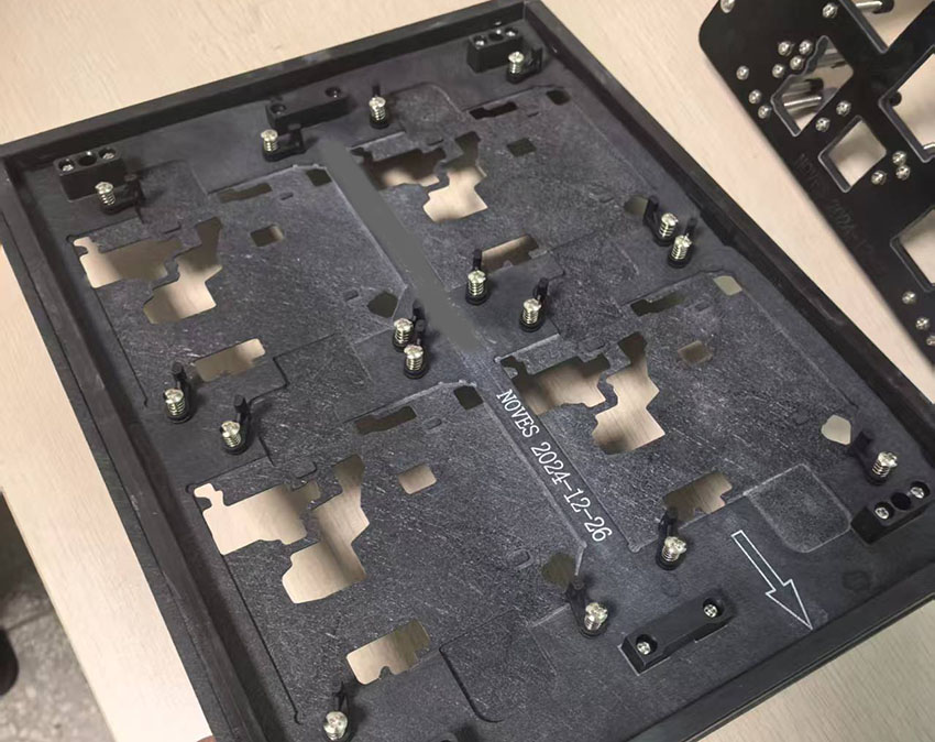
PCB Soldering Pallets & Carrier Frames

Engineered with Durostone material and CDM for Precision and Durability
Enhance PCB assembly efficiency with Noves’s premium PCB Soldering Pallets and Carrier Frames, crafted from advanced Durostone, CDM and Ricocel material. Designed for high-temperature stability and precision, these tools streamline PCBA soldering process, testing, and transport while protecting sensitive electronics.

- Key Features
一Extreme Heat Resistance:
Durostone,Ricocel and CDM materials withstand temperatures up to 260°C+ without warping, ensuring consistent performance in reflow ovens process, wave soldering process, and thermal cycling.
二Ultra-Low Thermal Expansion:
Wave soldering material reinforcement minimizes dimensional shifts (±0.05mm), maintaining precise alignment for PCB SMT components and micro-BGA soldering.
三Lightweight & Anti-Static:
30% lighter than aluminum with built-in ESD protection (10⁶–10⁹ Ω surface resistance), reducing static risks during handling.
四Customizable Design:
Laser-cut fiducial marks, tool-free clamps, and modular frames adapt to PCB sizes from 50x50mm to 450x450mm.
五Chemical Resistance:
Resists flux, solvents, and cleaning agents for long-term use in harsh environments during the PCB wave soldering production process.

- Applications
PCB Reflow/Wave Soldering: Ensure even heat distribution for defect-free joints.
- Automated SMT Lines: Secure PCBs during pick-and-place and inspection.
- Functional Testing: Stabilize boards during in-circuit (ICT) or boundary-scan tests.
- Multi-Batch Processing: Stackable frames optimize conveyor workflows.

Technical Specifications
- Materials: Durostone (high-temperature base), CDM (ceramic-composite surface layer), Wave solder pallet material, Noves material.
- Max Load: 8kg per pallet

The pallet design will be free of charge for customers. The below files are required for the pallet design:
1. 2D drawing (Dwg or PDF) or 3D drawing (step or Igs ) of the wave solder pallets
2. Gerber files of PCB bare board + Loaded PCB sample (PCB board with electronic components)
3. We will make the drawing for customer approval within 48 hours of receiving the files.
4. The photos of the PCBA in both sizes.
5. The production will be finished within 3-5 days after the customer approves the pallet drawing.
Please contact us any time by Email:[email protected]


